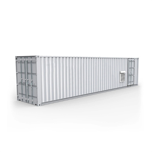
Multicrystalline 330w photovoltaic panel silicon wafer size

Review of multicrystalline silicon wafer solar cell processing
(a).Multicrystalline silicon wafer; (b). Boundary between crystals [2]. 2. Processing of Multicrystalline Silicon Solar Cells 2.1. Silicon Wafer Preparation Multicrystalline silicon is

330W 340W 350W Standard Polycrystalline Solar Panel
As one of the leading 330w 340w 350w standard polycrystalline solar panel manufacturers and suppliers in China, we warmly welcome you to wholesale high quality Mono Solar Panel made
Solar Panel Sizes And Wattage | Sizing, Dimensions
The number of solar panels x output = Solar system size. 20 x 330W panels = 6,600 W or 6.6kW solar system. The physical size of the solar panel; are based on the larger 180 and 210mm wafer (based silicon cells

Silicon feedstock for the multi-crystalline photovoltaic industry
The major results of this study are summarised in Fig. 3, showing that multi-crystalline silicon technology, currently already at the lowest direct production costs of 2.10

Photovoltaic recycling: enhancing silicon wafer recovery process
The rapid proliferation of photovoltaic (PV) modules globally has led to a significant increase in solar waste production, projected to reach 60–78 million tonnes by
Waaree (WS-330/ 24V) 330 Wp Polycrystalline Solar PV Module
Polycrystalline solar panel: Polycrystalline or multicrystalline solar panels are solar panels that consist of several crystals of silicon in a single PV cell. Several fragments of silicon are melted

Life Cycle Assessment of Crystalline Silicon Wafers for Photovoltaic
Life Cycle Assessment of Crystalline Silicon Wafers for Photovoltaic Power Generation Mingyang Fan1 & Zhiqiang Yu1,2,3 & Wenhui Ma1,2,3 & Luyao Li1 Received: 22 April 2020 /Accepted:
Detection and analysis of micro-cracks in multi-crystalline silicon
Conference: Photovoltaic Specialists Conference (PVSC), 2011 37th IEEEPhotovoltaic Specialists Conference (PVSC), 2011 37th IEEE

Status and perspectives of crystalline silicon photovoltaics in
With a typical wafer thickness of 170 µm, in 2020, the selling price of high-quality wafers on the spot market was in the range US$0.13–0.18 per wafer for multi-crystalline
Etching methods for texturing industrial multi-crystalline silicon
Multi-crystalline silicon (mc-Si) and mono crystalline silicon (c-Si) wafer based solar cells contribute ∼ 30% and ∼ 65%, respectively to the world wide PV panel installation
Effect of Additives on Making Texture Surface on Multicrystalline
In the production of multicrystalline silicon solar cell, diamond wire sawing method (DWS) is an important technique, which has already completely replaced multiwire

Life cycle assessment for a grid-connected multi-crystalline silicon
The solar panel of the PV system was assembled with twelve multi-purposed solar modules made up with polycrystalline (mc-Si) cells which were connected in series to
Polycrystalline silicon
Left side: solar cells made of polycrystalline silicon Right side: polysilicon rod (top) and chunks (bottom). Polycrystalline silicon, or multicrystalline silicon, also called polysilicon, poly-Si, or mc-Si, is a high purity, polycrystalline form of silicon,

Grain Boundaries in Multicrystalline Silicon | SpringerLink
Classification and Types of Grain Boundaries. In the previous chapters of this handbook, e.g., Chaps. 17, "Metal Impurities and Gettering in Crystalline Silicon" or 18,
Panasonic HIT KURO Series 330W All Black Hybrid Solar Panel
Panasonic HIT KURO Series 330W All Black Hybrid Solar Panel. £199.99 (ex. VAT) £239.99 (inc. VAT solar cells is made of a thin mono crystalline silicon wafer surrounded by ultra-thin

The emergence of high-performance multi-crystalline silicon in
The solar photovoltaic (PV) market has increased dramatically over the last decade. In 2015, the annual PV installation was over 50 GW, and the solar cells made from

Silicon crystal growth for PV solar cells | SGL Carbon
Silicon based photovoltaics relies on either mono- or multi-crystalline silicon crystal growth. Silicon wafers are the foundation of all Si solar cells. These are connected to PV modules after
Panasonic HIT KURO Series 330W All Black Hybrid Solar Panel
Less dirt on the panel means more sunlight getting through to generate power. Even at high temperatures, the HIT solar cell can maintain higher efficiency than a conventional crystalline

Solar Wafer M12 M10 M9 M6 G1 M4 M2
The larger the size, the higher the power and the lower the cost, leading the silicon industry to continue to introduce large size wafers, from M2, M4, G1, M6 to M12(G12). Before 2010,

Multi-crystalline Silicon | UniversityWafer, Inc.
The global crystalline silicon photovoltaic market has been segmented by type, end-user, geography, and industry. It has been projected that the world crystalline silicon photovoltaic

The Influence of Wire Sawing Process on Mono
Request PDF | On Jan 1, 2008, A Bohne and others published The Influence of Wire Sawing Process on Mono- and Multicrystalline Silicon Wafers | Find, read and cite all the research you

Why are monocrystalline wafers increasing in size?
Traditionally, monocrystalline silicon wafers before 2010 were classified as small-size with 125mm x 125mm width (164mm silicon ingot diameter) and only a small number at 156mm x 156mm (200mm
Solar Wafer M12 M10 M9 M6 G1 M4 M2
After 2010, 156mm x 156mm wafers increasingly became the popular choice (lower cost per-watt) for p-Type monocrystalline and multicrystalline wafer sizes. By the end of 2013, a number of

Impact of silicon wafer thickness on photovoltaic performance of
Author affiliations. 1 Research Center for Photovoltaics, National Institute of Advanced Industrial Science and Technology (AIST), Tsukuba, Ibrakaki 305-8568, Japan. 2

Status and perspectives of crystalline silicon photovoltaics in
Crystalline silicon solar cells are today''s main photovoltaic technology, enabling the production of electricity with minimal carbon emissions and at an unprecedented low cost.

Life-cycle assessment of multi-crystalline photovoltaic (PV)
In fact, for the PV industry, apart from the process of polycrystalline silicon production, other processes, such as quartz mining, metallurgical silicon production, cell and

Life cycle assessment of multicrystalline silicon photovoltaic cell
The sites reported a production of approximately 300 t/year of multi-crystal silicon, 3.6 × 10 7 m 2 /year of solar glass, 80 MW/year of PV wafer, and 120 MWp/year of PV
High quality multi-crystalline silicon wafer by grain size control
In recent year, efficiency of multi-crystalline silicon (mc) solar cell had large improvement due to better quality of wafer source. In continental thought, grain boundaries and dislocations are act

Pollutant payback time and environmental impact of Chinese multi
China holds an important share of the world photovoltaic industry. In 2015, the Chinese production yields of solar-grade silicon, silicon wafers, silicon cells, and photovoltaic

Multicrystalline Wafer
Most solar modules produced during 2004 used multicrystalline silicon wafers rather than monocrystalline ones. Grains are generally much larger than the wafer thickness (0.3 mm) and

Multicrystalline Silicon Cell
Polycrystalline silicon or multicrystalline silicon cells are manufactured by solidifying the large block of molten silicon to orient crystals in the fixed direction producing cast square ingots of
Related Contents
- Photovoltaic panel silicon wafer size specifications
- Photovoltaic panel silicon wafer pad manufacturer
- Single crystal silicon photovoltaic panel size and weight table
- Photovoltaic silicon panel size parameters
- What is the thickness of the photovoltaic panel silicon wafer
- Photovoltaic monocrystalline silicon panel market
- Double-glass photovoltaic panel size specifications
- Chint 585 photovoltaic panel size
- Photovoltaic silicon panel composition
- Yingli Inergy photovoltaic panel size
- Photovoltaic 650 panel size and weight table
- Photovoltaic panel DC power size